
 KOR
KOR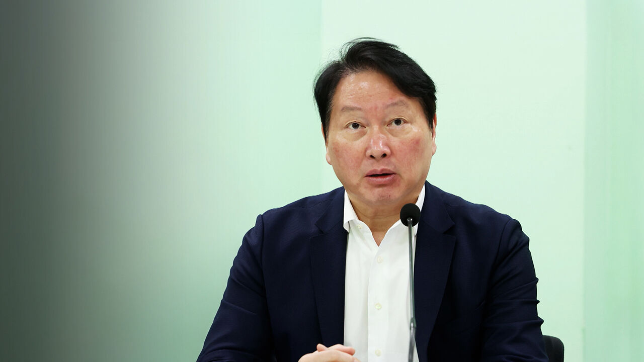
▲ SK Group Chairman Chey Tae-won
As SK Group Chairman Chey Tae-won revealed that Japan is being considered as a potential location for semiconductor investment, analysts suggest that local government support and the ecosystem for materials, parts, and equipment (MPE) likely played a significant role in the decision.
With expanding production capacity to address the prolonged surge in memory demand becoming the industry's top priority, Japan also offers favorable conditions for broadening the global supply chain.
In addition, given that Chairman Chey has already announced aggressive investment plans in the United States and South Korea, his global efforts to secure additional production hubs are expected to continue going forward.
According to the industry, Chairman Chey recently hinted at the possibility of joint production with Kioxia, a Japanese NAND flash memory manufacturer, during an interview with the Asahi Shimbun, describing it as "one option."
He also raised the possibility of various forms of cooperation, including research and development (R&D) and supply chain sharing.
It has been reported that investments in production facilities within Japan are also being examined from multiple perspectives.
In fact, Japan is attracting attention from global companies by actively supporting local investments by overseas semiconductor firms—such as TSMC and Micron—at the government level while rebuilding its semiconductor supply chain.
A robust materials, parts, and equipment ecosystem is another advantageous condition for semiconductor investment.
Miyagi Prefecture in Japan, which has been cited as a prominent candidate location, is densely populated with MPE companies and an industry-academia-research R&D ecosystem, spearheaded by Tokyo Electron, a leading global semiconductor etching equipment manufacturer.
Many of these companies are suppliers or customers of SK Hynix, establishing conditions to operate as a unified ecosystem.
Chairman Chey's consideration of investment in Japan is also in line with his principle of investing wherever conditions are favorable.
During a press conference held in Jeju last July, Chairman Chey emphasized regarding the semiconductor investment plans, "The current situation is that we are trying to build wherever we can build," adding, "Searching the world to prioritize where we can do it best, fastest, and on the largest scale, and building quickly has become the lifeline of South Korea's semiconductor industry."
This aggressive investment plan stems from the judgment that the increase in memory demand is a structural change rather than a temporary phenomenon.
At a recent press conference following SK Hynix's listing on Nasdaq, Chairman Chey stated, "When I go to Japan, they say we are reviewing a Japanese plant; when I go to the U.S., they say we are reviewing a U.S. plant, but we are at a point where even the maximum investment would not be enough."
Mentioning the accelerating pursuit by the Chinese semiconductor industry, he expressed frustration, saying, "SK Hynix must move 10 times faster than in the past."
"That is the most difficult homework we face right now."
Indeed, while SK Hynix has led the artificial intelligence (AI) semiconductor market with its competitiveness in high-bandwidth memory (HBM) technology, timely and stable supply of the memory required by customers has now emerged as a new battlefield.
Amid forecasts that securing additional bases both domestically and internationally will continue, Japan is being reviewed as one of several investment candidates for this purpose.
Recently, Chairman Chey revealed plans to double total wafer production capacity within the next five years.
Accordingly, large-scale production facility investments are currently underway in South Korea, centered around the Yongin Semiconductor Cluster and Cheongju.
SK has also announced plans to significantly accelerate the construction schedule of the Yongin Semiconductor Cluster and expand its production belt to Cheongju and the southwestern region.
At the same time, following the establishment of an advanced packaging production base for next-generation HBM in West Lafayette, Indiana, U.S., the possibility of additional investment remains open.
An industry insider said, "The current concern for SK Hynix is not just a matter of whether to build a single plant in Japan, but how to handle the explosive AI semiconductor demand expected over the next several years," adding, "Reviewing various options in global supply chains, including the U.S. and Japan, while maintaining South Korea as the core production base should be viewed as a strategic consideration to secure production capacity in the AI era."
※ Please note: This article was translated by AI and may contain errors.


 Video News
 Video News
 Video News
 Video News
 Video News