
 KOR
KOR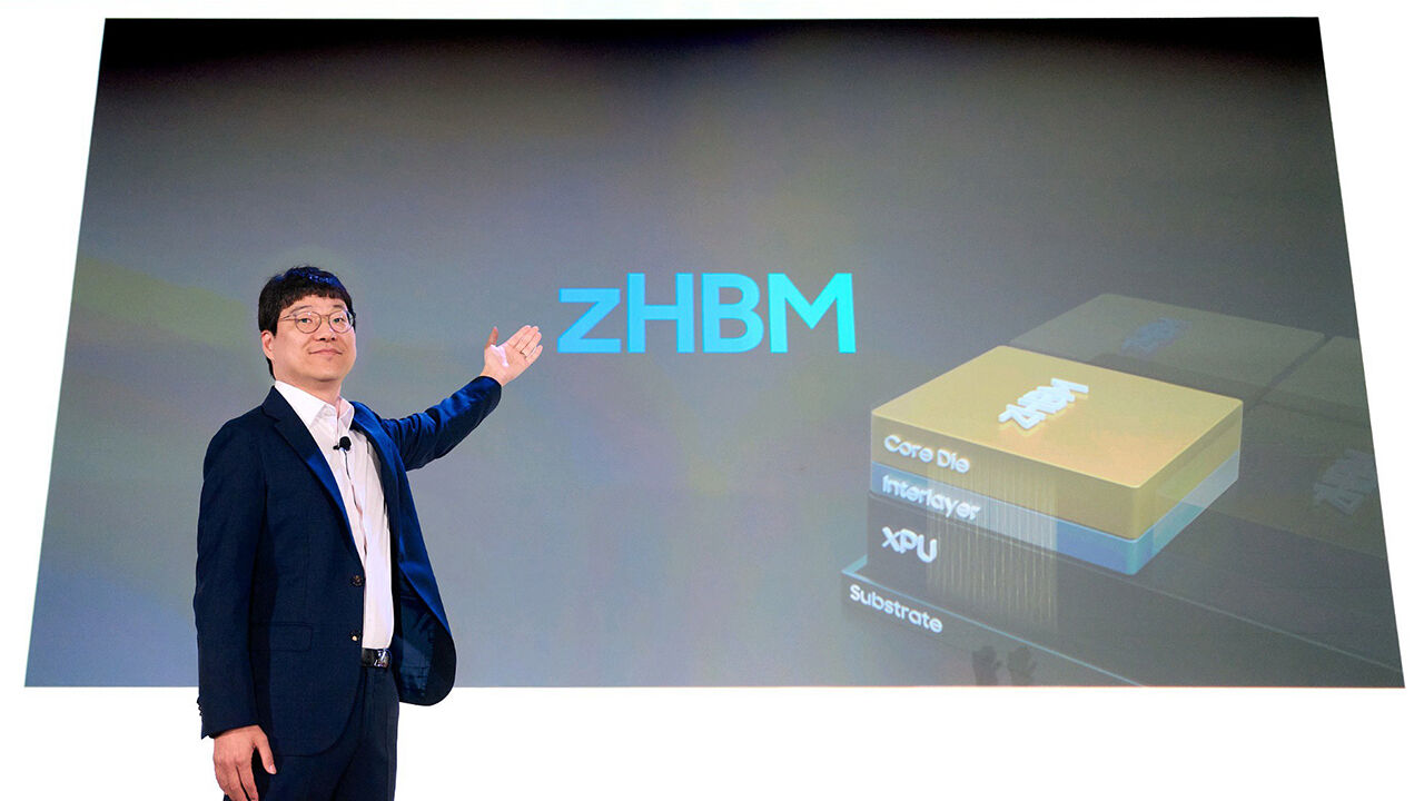
▲ Kim Kyoung-ryun, Vice President at Samsung Electronics, introduces 'zHBM'.
The main focus at "FMS 2026," a memory semiconductor event that opened on the 4th (local time) at the Santa Clara Convention Center in California, USA, was on how to overcome the "Memory Wall," which has emerged as a new limitation in the artificial intelligence (AI) era.
This is because as AI evolves beyond simply answering human questions into an "AI agent" stage where it plans and executes tasks on its own, the importance of memory in storing and transmitting data is growing increasingly crucial.
No matter how exceptional the performance of an AI semiconductor is, its computing power cannot be fully utilized if the necessary data is not supplied in a timely manner.
It is similar to how even the smartest brain has difficulty functioning properly if the data it needs to process arrives late.
As a solution to cross this memory wall, Samsung Electronics presented a three-dimensional technology that breaks away from the conventional planar structure by stacking memory vertically.
Currently, High Bandwidth Memory, or HBM, is placed alongside AI accelerators such as Graphics Processing Units (GPUs) to exchange data.
While this minimizes the distance between memory and processing units to increase data processing speed, limitations such as data transfer time and power consumption have remained due to physical space constraints.
The "zHBM" unveiled by Samsung on this day applies a method of stacking HBM directly on top of the GPU to solve this problem.
It is a concept aimed at reducing the distance data travels to virtually "zero."
According to Samsung Electronics, zHBM is projected to achieve up to 8 times the performance and up to 3 times the power efficiency compared to the 8th-generation HBM5, which is expected to go into mass production in 2028.
Kim Kyoung-ryun, Vice President of the DRAM Development Office at Samsung Electronics, emphasized, "Everyone knows that current HBM technology will hit a limit in the next few years," adding, "When considering what technology will break through this, 3D is the only answer."
However, there is a concern that stacking memory on top of an AI accelerator could generate significant heat.
To address this, Samsung chose to reduce the number of DRAM stacking layers compared to regular HBM.
Vice President Kim added, "Looking at what our customers currently want, there is stronger demand for solving heating and bandwidth issues."
SK Hynix also unveiled a similar direction of 3D memory technology.
SK Hynix's "G0.5" is a product targeting the gap between SRAM, which features high bandwidth but small capacity, and conventional HBM, which provides large capacity.
Given that SRAM is considered G0 and conventional HBM is G1, the name G0.5 was given to signify the intermediate stage.
Both companies also presented ways to utilize NAND flash as next-generation AI memory.
As hyperscale AI operates and generates massive amounts of tokens—meaning a sharp increase in the volume of data generated during AI computation—it has become difficult to store all of them in expensive DRAM.
Consequently, they have proposed NAND flash, which is slower than DRAM but lower in price and larger in storage capacity, as a new alternative.
SK Hynix introduced High Bandwidth NAND (HBF) as a "G1.5" product that bridges the gap between HBM and DRAM.
Samsung Electronics also unveiled "zNAND-O," which vertically stacks NAND flash and combines it with a Neural Processing Unit (NPU).
However, there is a difference in the target markets for the two products.
While SK Hynix's HBF targets server environments such as data centers, Samsung's zNAND-O focuses on "on-device AI," which processes AI directly within devices like smartphones.
Although both Samsung Electronics and SK Hynix chose the technology of stacking memory vertically, their market approach strategies differed.
Samsung, which possesses not only memory but also semiconductor contract manufacturing, or foundry operations, emphasized its integrated competitiveness capable of providing everything from design and production to advanced packaging at once.
Furthermore, based on the fact that it manufactures personal AI devices such as Galaxy smartphones, the company plans to aggressively target the on-device AI market that executes AI directly inside devices.
On the other hand, SK Hynix put forward a strategy to expand the market through open cooperation and standardization.
SK Hynix's disclosure of the HBF standard specifications—developed alongside SanDisk and others—through OCP, the world's largest open data center technology collaboration organization, is part of this strategy.
Attention is focused on whether the next-generation memory technologies presented by Samsung Electronics and SK Hynix can become the core competitive edge that determines leadership in the upcoming AI era.
(Photo provided by Samsung Electronics, Yonhap News)
※ Please note: This article was translated by AI and may contain errors.





 Video News
 Video News